Printed Circuit Board Manufacturing
Printed circuit board manufacturing is a process that consists of various processes including Tin plating, Reverse engineering, and Electrical tests. Each of these processes involves its own unique challenges and advantages. Hence, you need to choose the correct process for your specific needs.
Printing circuit board design
Printed circuit boards are vital to the proper functioning of electronic devices. They are used in a wide range of products including computers, mobile phones, CAT scans, X-rays, radios, heart monitors, and control tower instrumentation.
Printed circuit board fabrication requires certain levels of efficiency and quality. Several tests are conducted throughout the manufacturing process to ensure the functional reliability of the completed boards. Some boards are also subjected to extremes of heat and humidity.
The first step in the PCB design and manufacturing process is to analyze the requirement. After that, the appropriate components are selected. Then, the circuit pattern is derived with the help of special software. It is then exported in a suitable format.
Substrate
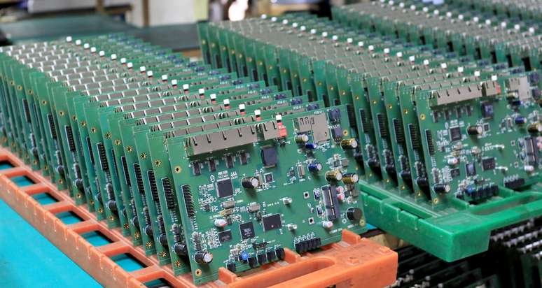
Printed circuit board manufacturing is the process of creating a self-contained module of electronic components. The basic PCB is made up of a thin layer of copper foil and insulating layers. These boards are found in radios and household electrical devices. They are also used in more sophisticated computer systems.
Printed circuit boards are manufactured using a variety of techniques. These methods produce boards with different functions. There are two main types of processes, a subtractive and an additive method.
A subtractive process involves the application of photoresist to the substrate. A photoresist is a polymer that becomes soluble when exposed to ultraviolet light. This enables the material to be selectively removed from the surface of the substrate.
Tin plating
Printed circuit boards are used to connect electronic components in electronic equipment. The process of PCB tinning involves depositing a thin layer of tin onto a copper base. The tin layer is used to protect the copper from oxidation and provides a flat surface for wire bonding.
Tin plating in printed circuit board manufacturing requires extreme precautions. The PCB needs to be pre-treated before it is placed into the tin bath. The circuit board should then be washed to remove any plating salts, followed by drying. The circuit board can be forced air dried, or heated in a warm oven.
The pH level of the tin bath should be between pH 3 and 8. The tin must be pure and free of defects. A solder mask must also be applied. The solder mask should not change color or fall off.
Reverse engineering
Printed circuit boards (PCBs) offer an electrical route between electronic components. They have thin copper foil conductive layers that are laminated together.
Aside from the obvious function of PCBs, they are also used for a variety of other purposes. For instance, a PCB can be used to make a new product. It can also be used to improve or repair an existing PCB.
Reverse engineering is a technique that can be used to extract design information from a PCB. It involves using a number of tools to deconstruct components on a PCB. It can be done manually or with a computerized system.
The most basic process is to photograph the PCB on both sides. This will minimize the reflection of light from the PCB masks. The images can then be uploaded to a reverse engineering program.
Aligning the layers
Getting the layers in printed circuit board manufacturing right is a challenge. This is because there are many factors that can cause interlayer misalignment. The good news is that there are techniques to reduce this type of error. Using a high-precision alignment exposure machine is one way to accomplish this.
The process of getting the layers in printed circuit board manufacturing right involves a number of steps. First, the PCB board is assembled on a heavy steel table. Each layer is then pressed against the other. This is aided by metal clamps.
Next, a special press table is used. The computer on the press determines the pressure points and automatically heats the copper. This is followed by copper deposition and plating. After this, the board takes shape.
Electrical tests
Performing electrical tests on printed circuit boards is a common process during the manufacturing process. These tests are used to determine the integrity of the board, including traces and pad connections. They also help to identify potential problems in the design.
In addition, they can be used to test for isolation between traces and pads. These types of tests are typically conducted before the board is delivered.
If you need PCB’s reated for your project, contact https://www.avanticircuits.com today.


